A team of researchers has developed a new silicon construction technique that could potentially improve the affordability and reliability of building quantum computers.
The new technique — jointly developed by researchers from Australia’s University of Melbourne, University of New South Wales (UNSW) and RMIT, and Germany’s Helmholtz-Zentrum Dresden-Rossendorf and Leibniz Institute of Surface Engineering — involves precisely embedding single atoms one-by-one in silicon wafers.
According to the researchers, the technique, which has been published in an Advanced Materials paper, takes advantage of the precision of the atomic microscope, which has a sharp cantilever that “touches” the surface of a chip with a positioning accuracy of just half a nanometre, which is about the same space between atoms in a silicon crystal.
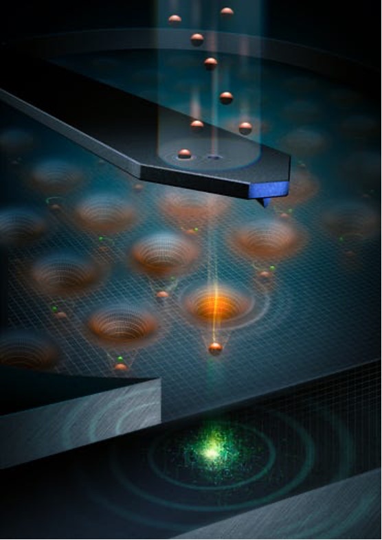
The researchers described how a tiny hole was drilled in the cantilever, so that when it was showered with phosphorous atoms, one would occasionally drop through the hole and embed in the silicon substrate.
A key aspect of this was knowing precisely when an atom was embedded in the substrate so the cantilever could move to the next precise position on the array.
The paper noted that up until now, implanting atoms in silicon has been a haphazard process as when a silicon chip gets showered with phosphorous, an atom would drop in a random pattern, like raindrops on a window. However, the team discovered that it could identify the preciseness through a “click” sound that occurs when an atom drops into the silicon crystal.
“One atom colliding with a piece of silicon makes a very faint click, but we have invented very sensitive electronics used to detect the click, it’s much amplified and gives a loud signal, a loud and reliable signal,” University of Melbourne professor and lead author David Jamieson said.
“That allows us to be very confident of our method. We can say, ‘Oh, there was a click. An atom just arrived. Now we can move the cantilever to the next spot and wait for the next atom.'”
The researchers used equipment including sensitive x-ray detectors, an atomic force microscope that was originally developed for the Rosetta space mission, along with a computer model for the trajectory of ions implanted into silicon, to develop the technique.
Co-author and UNSW Scientia professor Andrea Morello said using this precision and new technique, it would be possible to create a qubit “chip”, which can then be used in experiments to test designs for large scale devices.
“This will allow us to engineer the quantum logic operations between large arrays of individual atoms, retaining highly accurate operations across the whole processor,” he said.
“Instead of implanting many atoms in random locations and selecting the ones that work best, they will now be placed in an orderly array, similar to the transistors in conventional semiconductors computer chips.”
Jamieson added some of the potential large-scale quantum devices that could be developed using the design include unbreakable cryptography and computational drug design, such as rapid development of vaccines.
“We believe we ultimately could make large-scale machines based on single atom quantum bits by using our method and taking advantage of the manufacturing techniques that the semiconductor industry has perfected,” he said.
Via ZDNet, authored by Aimee Chanthadavong, 13 January 2022